The DP receiver (DPRX) receives video from a DP source device. The core consists of two
main layers; the policy maker (PM) and link layer (LNK). The policy maker is responsible for
communication with the upstream DP source device, training the link and controlling the link
layer. The link layer handles the (video) data transport.
The DPRX diagram is shown in figure 1.
Figure 1: DPRX diagram
| Name | Type | Description | Values |
|---|---|---|---|
| P_VENDOR | String | Vendor | AMD, ALTERA, LSC |
| P_BEAT | Integer | Beat value | 50 |
| P_SDP | Bool | SDP support | 0, 1 |
| P_LANES | Integer | Number of lanes | 2, 4 |
| P_SPL | Integer | Symbols per lane | 2, 4 |
| P_PPC | Integer | Pixels per clock | 2, 4 |
| P_BPC | Integer | Bits per component | 8, 10 |
| P_VID_DAT | Integer | Video data width | 48, 64, 96, 120 |
| Name | Clock | Description | Width |
|---|---|---|---|
| SYS_RST_IN | SYS_CLK | System reset | 1 |
| SYS_CLK_IN | SYS_CLK | System clock (50 MHz) | 1 |
| HOST_IF | SYS_CLK | Host interface | - |
| HOST_IRQ_OUT | SYS_CLK | Host interrupt | 1 |
| AUX_EN_OUT | SYS_CLK | AUX channel enable | 1 |
| AUX_TX_OUT | SYS_CLK | AUX channel transmit | 1 |
| AUX_RX_IN | SYS_CLK | AUX channel receive | 1 |
| HPD_OUT | SYS_CLK | Hot Plug Detect | 1 |
| HB_OUT | SYS_CLK | Heartbeat | 1 |
| LNK_CLK_IN | LNK_CLK | Link clock | 1 |
| LNK_DAT_IN | LNK_CLK | Link data | P_LANES * P_SPL * 9 |
| LNK_SYNC_OUT | LNK_CLK | Link sync | 1 |
| LNK_VBID_OUT | LNK_CLK | Vertical Blanking ID | 1 |
| VID_CLK_IN | VID_CLK | Video clock | 1 |
| VID_RDY_IN | VID_CLK | Video ready | 1 |
| VID_SOF_OUT | VID_CLK | Video start of frame | 1 |
| VID_EOL_OUT | VID_CLK | Video end of line | 1 |
| VID_DAT_OUT | VID_CLK | Video data | P_VID |
| VID_VLD_OUT | VID_CLK | Video valid | 1 |
| SDP_CLK_IN | SDP_CLK | Secondary data packet clock | 1 |
| SDP_SOP_OUT | SDP_CLK | Secondary data packet start | 1 |
| SDP_EOP_OUT | SDP_CLK | Secondary data packet end | 1 |
| SDP_DAT_OUT | SDP_CLK | Secondary data packet data | 32 |
| SDP_VLD_OUT | SDP_CLK | Secondary data packet valid | 1 |
The link interface connects the DPRX with the FPGA serdes. The link interface signals have the prefix LNK_. The link clock (LNK_CLK_IN) is generated by the FPGA serdes.
The link clock frequency depends on the actual link rate. The link data (LNK_DAT_IN) is directly coming from the FPGA serdes. See the DP reference design for the mapping.
The link clock for the various link rates are shown in the table below.
The link clock is generated by the FPGA serdes.
| Link rate | Symbols per clock | Link clock |
|---|---|---|
| RBR - 1.62 | 2 | 81 |
| RBR - 1.62 | 4 | 40.5 |
| HBR - 2.7 | 2 | 135 |
| HBR - 2.7 | 4 | 67.5 |
| HBR2 - 5.4 | 2 | 270 |
| HBR2 - 5.4 | 4 | 135 |
| HBR3 - 8.1 | 2 | 405 |
| HBR3 - 8.1 | 4 | 202.5 |
The DPRX has an AXI-stream video interface. The interface can support 2 or 4 pixels per clock.
The video interface signals listed in the signal table have the prefix VID_. The video clock is driving the video interface.
The diagrams below show the waveform and pixel mappings of the various configurations.
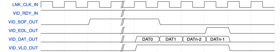
Figure 2: Video - waveform (click on the image to enlarge it)
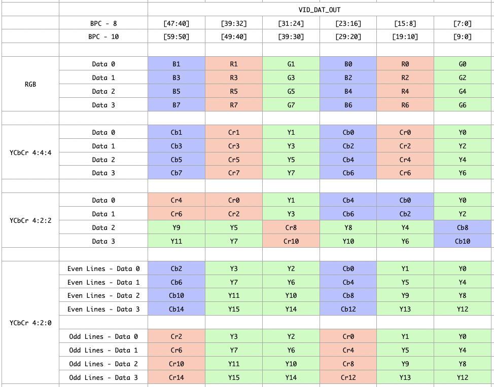
Figure 3: Video - 2 pixels per clock / 10 bits per component (click on the image to enlarge it)
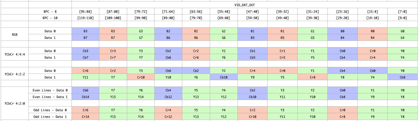
Figure 4: Video - 4 pixels per clock / 8 bits per component (click on the image to enlarge it)
The video toolbox (VTB) module VTB uses the LNK_SYNC_OUT signal to recover the video clock.
The external video clock generator (located on the Tentiva FMC board) generates the
video clock and is steered by the VTB clock recovery module.
The DPRX handles all secondary data packets and output through the SDP interface.
The SDP interface signals listed in the signal table have the prefix SDP_. The SDP interface is running at a free running clock (SDP_CLK_IN).
The DPRX has an internal FIFO to store some SDP packets. To prevent the FIFO from overflowing, the SDP clock needs to run faster than the link clock.
Figure 4 provides a waveform diagram, showing the timing and mapping of the SDP signals for an infoframe.
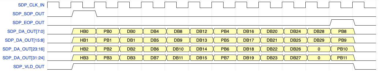
Figure 5: Video - 4 pixels per clock / 10 bits per component (click on the image to enlarge it)
Figure 5 shows the timing and mapping of a SDP audio packet.
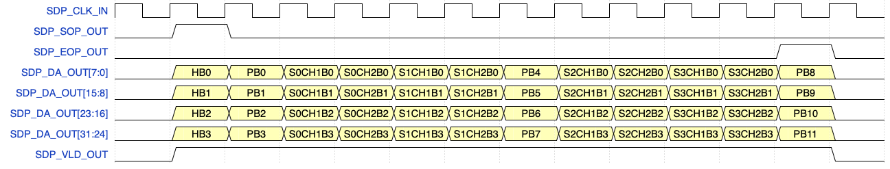
Figure 5: Video - 4 pixels per clock / 10 bits per component (click on the image to enlarge it)