Reference Design
Introduction
The reference design consists of the modules DisplayPort TX (DPTX), DisplayPort RX (DPRX), Video Toolbox (VTB), PHY and application. The block diagram is shown below. The VTB is a collection of video helper modules. It has a timing generator, colorbar generator, FIFO and video clock recovery. The reference design has two operation modes; colorbar and pass-through. In colorbar mode the test pattern, generated by the VTB, is transmitted by the DPTX to the DisplayPort sink device. When the pass-through mode is selected, the video coming from the DisplayPort source is captured by the DPRX. Then the video is forwarded to the DPTX through the VTB. The application has a RISC-V processor, memory (rom and ram) and a set of peripherals. The RISC-V processor runs the application code and DisplayPort IP-core host driver. The I2C peripheral is used to configure the external reference clock synthesizers (PHY and video clocks). The PHY registers are accessed through the DRP / LMMI / RCFG peripheral.

Figure 1: Reference design
Running
This paragraph describes how to run the reference design on the board.
The reference design uses the Tentiva board. Tentiva is a video FMC board with DisplayPort sink and source connectors. Mount the Tentiva board on the FMC HPC connector located on the FPGA development board. Use the plastic screws to secure the Tentiva board.
The reference design is available for the following platforms;
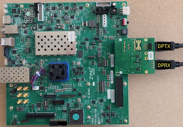
Figure 2: AMD ZCU102 board setup
FMC voltage
At power-up the ZCU102 system controller reads the FMC EEPROM and sets the FMC voltage (VADJ). The EEPROM on the Tentiva FMC baseboard has a different layout and as a result the ZCU102 system controller doens’t power the FMC voltage. For correct operation the FMC VADJ has to be set to 1.8V manually. Use the ZCU102 system controller GUI to set the FMC VADJ voltage.
Click here for more information on the ZCU102 system controller GUI.The FMC voltage can also be set through the UART. Click here for more information.
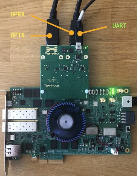
Figure 3: Intel DK-DEV-10CX220 board setup
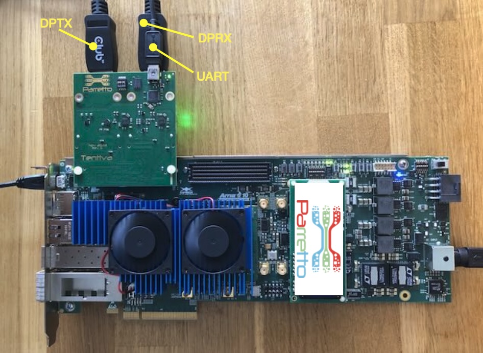
Figure 4: Intel DK-DEV-10AX115S board setup
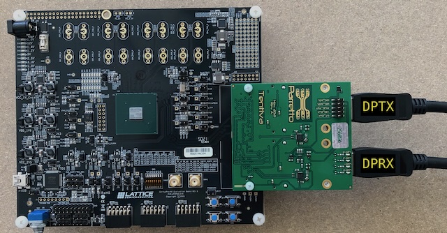
Figure 5: Lattice CertusPro-NX board setup
The jumpers JP1 (TXD_UART) and JP2 (RXD_UART) must be installed