Receiver
The HDMI receiver (HDMIRX) receives video from a HDMI source device. The core consists of two main layers; the system controller (SC) and link layer (LNK). The system controller is responsible for communication with the upstream HDMI source device and bring up the link. The link layer handles the (video) data transport.
Architecture
The system controller sits on the system clock and holds a small RISC-V core that runs the HDMI firmware. Everything below the clock domain boundary runs on the link clock. Link data from the FPGA serdes enters on the left and passes through three identical TMDS channels, one per data lane. What comes out of the channels is split in two: the video pixels go to the video block and out over the native video interface, the data island packets go to the packet block and out over the packet interface.
The two domains meet at a clock domain crossing that carries traffic in both directions. Configuration goes down, such as the scrambler enable. Status comes back up: the lock state of the word aligners, the decoders, the descramblers and the channel aligner, together with the video parameters the receiver has detected. That upward path is how the driver learns what the source is actually sending.
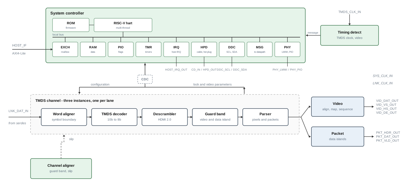
Figure 1: HDMI receiver architecture (click on the image to enlarge it)
-
System controller
prt_hdmi_sc_topA RISC-V core with its own ROM and RAM, running the firmware that brings up and manages the link: cable detect, the hot plug output, the DDC exchange that serves the EDID to the source, and the PHY controller. It talks to the application processor through a mailbox, and to the link layer through a message bus across the clock domain boundary.
-
Oversampler
prt_hdmirx_ovsKeeps one sample in two or four, so that a format whose line rate is below what the serdes can lock to is still received. The source sends every bit as many times, the link then runs at two or four times the rate the video needs, and this stage takes the video back out of it. The width of the link path does not change; the oversampling is in the time.
Which of the samples is kept does not matter. Any of them returns the transmitted bit stream at most one whole bit shifted, and a whole bit is precisely what the word aligner below already takes out by picking one of ten offsets - so there is no phase to search for and no feedback to build.
-
Link clock enable
prt_hdmirx_lnk_ckeProduces the one in one, one in two or one in four enable that the whole link domain runs on, so that every stage below sees one word per symbol whatever the link is doing. One generator serves the three channels and the video clock enable, so they cannot drift apart.
-
Word aligner
prt_hdmirx_tmds_walnFinds the symbol boundary in the incoming serial data of its lane. It reports its lock state to the system controller and accepts slip commands from the channel aligner.
-
TMDS decoder
prt_hdmirx_tmds_decTurns each 10-bit TMDS symbol back into its 8-bit character, and recovers the control and guard band information that goes with it.
-
Descrambler
prt_hdmirx_tmds_scrmUndoes the scrambling of the HDMI 2.0 specification, and reports its own lock state.
-
Guard band
prt_hdmirx_tmds_gbRegenerates the video and data island guard bands from the preamble and guard band inputs, so the parser knows where each period begins.
-
Parser
prt_hdmirx_tmds_parsSplits the stream into the two things that follow it: video pixels and data island packets.
-
Channel aligner
prt_hdmirx_calnThe three lanes do not necessarily arrive aligned. This block compares the video guard band of the channels and issues slip commands back to the word aligners until they line up.
-
Video
prt_hdmirx_vidAligns, maps and sequences the pixel data of the three channels into the native video interface, in the color space the source is sending.
-
Packet
prt_hdmirx_pktReassembles the data island packets and presents them on the packet interface, header and payload separately.
-
Timing detect
prt_hdmirx_tcdprt_hdmirx_vtdThe clock detector measures the incoming TMDS clock and the video timing detector measures the resolution being received. Both sit on the system clock next to the system controller and report to it over the message bus, which is how the driver learns what the source is sending. The video timing detector samples the sync signals from the link domain to do its counting.
| Name | Type | Description | Values |
|---|---|---|---|
| P_VENDOR | String | Vendor | LSC |
| P_BEAT | Integer | Beat value | 50 |
| P_SPL | Integer | Symbols per lane | 2, 4 |
| P_PPC | Integer | Pixels per clock | 2, 4 |
| P_BPC | Integer | Bits per component | 8 |
| Name | Clock | Description | Width |
|---|---|---|---|
| SYS_RST_IN | SYS_CLK | System reset | 1 |
| SYS_CLK_IN | SYS_CLK | System clock (50 MHz) | 1 |
| HOST_IF | SYS_CLK | Host interface | AXI4-Lite |
| HOST_IRQ_OUT | SYS_CLK | Host interrupt | 1 |
| CB_IN | SYS_CLK | Cable Detect | 1 |
| HPD_OUT | SYS_CLK | Hot Plug Detect | 1 |
| HB_OUT | SYS_CLK | Heartbeat | 1 |
| DDC_SCL_INOUT | SYS_CLK | Display Data Communication Clock | 1 |
| DDC_SDA_INOUT | SYS_CLK | Display Data Communication Data | 1 |
| TMDS_CLK_IN | - | TMDS clock input | 1 |
| LNK_CLK_IN | LNK_CLK | Link clock | 1 |
| LNK_DAT_IN | LNK_CLK | Link data | 3 * P_SPL * 10 |
| VID_VS_OUT | LNK_CLK | Video vertical sync | P_PPC |
| VID_HS_OUT | LNK_CLK | Video horizontal sync | P_PPC |
| VID_DAT_OUT | LNK_CLK | Video data | 3 * P_PPC * P_BPC |
| VID_G_OUT | LNK_CLK | Video green | P_PPC * P_BPC |
| VID_B_OUT | LNK_CLK | Video blue | P_PPC * P_BPC |
| VID_DE_OUT | LNK_CLK | Video data enable | P_PPC |
Clocking
The core uses two clock domains. The system clock (SYS_CLK, 50 MHz) drives the system controller and the host interface (AXI4-Lite). The link clock (LNK_CLK) drives the video and link interfaces and is derived from the pixel clock divided by the number of pixels per clock. The video interface therefore runs synchronously with the link layer.
Link Interface (LNK)
The link interface connects the HDMIRX with the FPGA serdes. The link interface signals have the prefix LNK_. The link clock (LNK_CLK_IN) is generated by the FPGA serdes. The link clock frequency depends on the actual video resolution. The link data (LNK_DAT_IN) is directly coming from the FPGA serdes.
Video Interface (VID)
The HDMIRX has a native video interface. The interface can support 2 or 4 pixels per clock. The video interface signals listed in the signal table have the prefix VID_. The pixel mapping of the video interface for each supported color space (RGB 4:4:4, YCbCr 4:4:4 and YCbCr 4:2:2) is described in the HDMI Mapping section.