Transmitter
The DP transmitter (DPTX) consists of two main layers: the policy maker (PM) and link layer (LNK). The policy maker is responsible for communication with the downstream DP sink device, training the link, and controlling the link layer.
The DPTX diagram is shown in Figure 1.
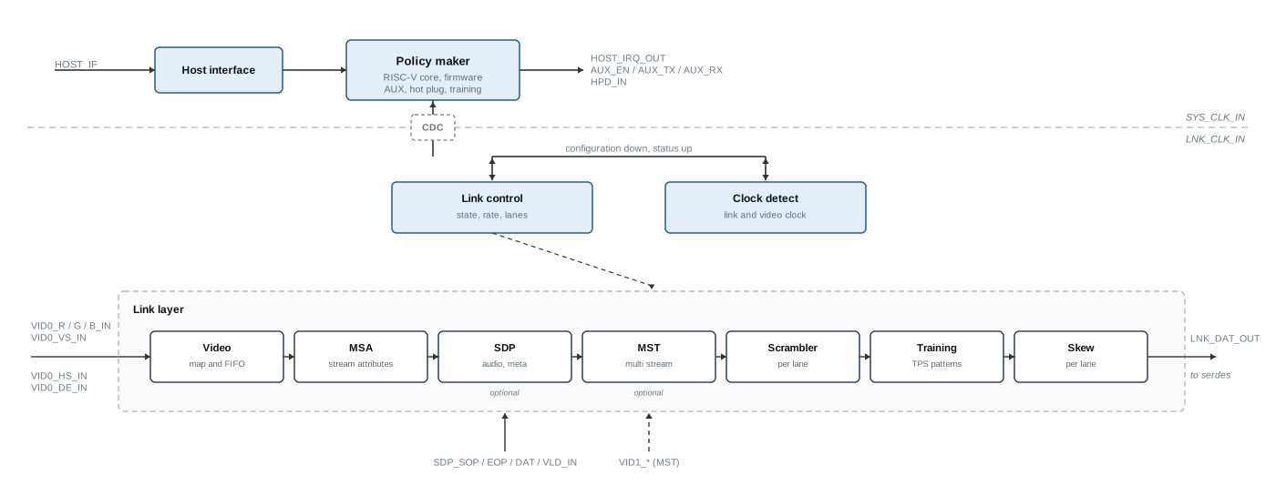
Figure 1: DPTX architecture (click on the image to enlarge it)
Architecture
The policy maker sits on the system clock. Everything below the clock domain boundary runs on the link clock. Video enters on the left, is mapped onto the lanes and dressed with the attributes and packets the standard asks for, and leaves as link data for the FPGA serdes. Link control drives every stage of the layer; the clock detectors only measure the incoming clocks and report what they find back to the policy maker.
-
Policy maker
prt_dp_pm_topA RISC-V core with its own ROM and RAM, running the firmware that owns the protocol: the AUX channel, hot plug detect, capability exchange and link training. It talks to the application processor through a mailbox, and to the link layer through a message bus across the clock domain boundary.
-
Link control
prt_dptx_ctlHolds the link state the policy maker has set — line rate, lane count, transport mode — and drives the stages of the link layer accordingly.
-
Video
prt_dptx_vidTakes the native video in, buffers it across into the link clock and maps the pixels onto the active lanes. The video FIFO absorbs the difference between the pixel rate and what the link can carry.
-
MSA
prt_dptx_msaInserts the main stream attributes: the timing and format description the sink needs in order to reconstruct the picture.
-
SDP
prt_dptx_sdpInserts the secondary data packets that carry audio and meta data, taken from the secondary packet interface. Built in only when the SDP parameter is enabled.
-
MST
prt_dptx_mstSplits the link into time slots so that more than one video stream can share it. Built in only when the MST parameter is enabled; in single stream mode the datapath passes straight through.
-
Scrambler
prt_dptx_scrmScrambles the symbols on each lane, as the DisplayPort specification requires.
-
Training
prt_dptx_trnReplaces the data with the training pattern sequences while the link is being brought up, under control of the policy maker, and hands the lanes back to normal traffic once training passes.
-
Skew
prt_dptx_skewApplies the inter-lane skew the specification prescribes before the symbols go to the serdes.
| Name | Type | Description | Values |
|---|---|---|---|
| P_VENDOR | String | Vendor | AMD, ALTERA, LSC |
| P_FAMILY | String | Family. Altera: AGX (Agilex), Lattice: LFCPNX | AGX, LFCPNX |
| P_BEAT | Integer | Beat value | 50 |
| P_MST | Bool | MST support | 0, 1 |
| P_SDP | Bool | SDP support | 0, 1 |
| P_LANES | Integer | Number of lanes | 2, 4 |
| P_SPL | Integer | Symbols per lane | 2, 4 |
| P_PPC | Integer | Pixels per clock | 2, 4 |
| P_BPC | Integer | Bits per component | 8, 10 |
| Name | Clock | Description | Width |
|---|---|---|---|
| SYS_RST_IN | SYS_CLK | System reset | 1 |
| SYS_CLK_IN | SYS_CLK | System clock (50 MHz) | 1 |
| APB_IF | SYS_CLK | Host interface | APB |
| HOST_IRQ_OUT | SYS_CLK | Host interrupt | 1 |
| AUX_EN_OUT | SYS_CLK | AUX channel enable | 1 |
| AUX_TX_OUT | SYS_CLK | AUX channel transmit | 1 |
| AUX_RX_IN | SYS_CLK | AUX channel receive | 1 |
| HPD_IN | SYS_CLK | Hot Plug Detect | 1 |
| HB_OUT | SYS_CLK | Heartbeat | 1 |
| VID0_CLK_IN | VID_CLK | Video clock (stream 0) | 1 |
| VID0_CKE_IN | VID_CLK | Video clock enable (stream 0) | 1 |
| VID0_VS_IN | VID_CLK | Video vertical sync (stream 0) | 1 |
| VID0_HS_IN | VID_CLK | Video horizontal sync (stream 0) | 1 |
| VID0_DAT_IN | VID_CLK | Video data (stream 0). Per pixel {R / Cr, B / Cb, G / Y} | 3 * P_PPC * P_BPC |
| VID0_DE_IN | VID_CLK | Video data enable (stream 0) | 1 |
| SDP_CLK_IN | SYS_CLK | Secondary data packet clock | 1 |
| SDP_RDY_OUT | SDP_CLK | Secondary data packet ready | 1 |
| SDP_SOP_IN | SDP_CLK | Secondary data packet start | 1 |
| SDP_EOP_IN | SDP_CLK | Secondary data packet end | 1 |
| SDP_DAT_IN | SDP_CLK | Secondary data packet data | 32 |
| SDP_VLD_IN | SDP_CLK | Secondary data packet valid | 1 |
| VID1_CLK_IN | VID_CLK | Video clock (stream 1, MST only) | 1 |
| VID1_CKE_IN | VID_CLK | Video clock enable (stream 1, MST only) | 1 |
| VID1_VS_IN | VID_CLK | Video vertical sync (stream 1, MST only) | 1 |
| VID1_HS_IN | VID_CLK | Video horizontal sync (stream 1, MST only) | 1 |
| VID1_DAT_IN | VID_CLK | Video data (stream 1, MST only). Per pixel {R / Cr, B / Cb, G / Y} | 3 * P_PPC * P_BPC |
| VID1_DE_IN | VID_CLK | Video data enable (stream 1, MST only) | 1 |
| LNK_CLK_IN | LNK_CLK | Link clock | 1 |
| LNK_DAT_OUT | LNK_CLK | Link data | P_LANES * P_SPL * 11 |
Video Interface
The DPTX has a native video interface and supports 2 or 4 pixels per clock. The video interface signals listed in the signal table have the prefix VID0_ and are high active. The second stream (VID1_) is only used with MST. All the pixels of a clock come in on one data bus, VID0_DAT_IN, of 3 * P_PPC * P_BPC bits. Each pixel takes 3 * P_BPC bits, with green / Y in the lowest bits, then blue / Cb and then red / Cr: per pixel {R / Cr, B / Cb, G / Y}. Pixel 0 is in the lowest bits of the bus. YCbCr 4:4:4 has the same mapping as RGB. The DPTX only takes the video signals in on clocks where the clock enable VID0_CKE_IN is high. Tie it high when the video clock is exactly the pixel clock divided by the pixels per clock; drive it from a clock enable DCO when the video clock runs faster. The video clock (VID0_CLK_IN) runs at the pixel clock divided by the pixels per clock (2 or 4). For example with video resolution 1080p60 the pixel clock is 148.5 MHz. In 2 pixels per clock configuration the video clock runs at 74.25 MHz. It has a frequency of 37.125 MHz in 4 pixels per clock. The video clock must be stable and is generated by a PLL. The DPTX can support any video timing as long as the horizontal video timing is dividable by the number of pixels per clock (2 or 4). Figure 2 shows the video timing. Each data word (D0 to Dn) carries P_PPC pixels; how the pixels are mapped within a word is shown in figures 3 and 4.

Figure 2: Video timing (click on the image to enlarge it)
Video mapping
The video data input VID0_DAT_IN is 3 * P_PPC * P_BPC bits wide and carries per pixel {R / Cr, B / Cb, G / Y}, with green / Y in the lowest bits. Pixel 0 is the first pixel of the group and sits in the lowest bits of the bus. The IP-core supports RGB 4:4:4 and YCbCr 4:4:4. Both share the same bit layout: Cr takes the place of red, Y the place of green and Cb the place of blue. With 8 bits per component in a core built for 10 bits per component (P_BPC = 10), the components are MSB-aligned in each 10-bit field and the 2 lowest bits are unused. The second stream (VID1_DAT_IN, MST only) has the same mapping.

Figure 3: Video mapping - 2 pixels per clock (click on the image to enlarge it)

Figure 4: Video mapping - 4 pixels per clock (click on the image to enlarge it)
Video clocking
The transmitter can support any video resolution. The table lists the video clocks for SD/HD video resolutions. The video clock is generated by the user.
| Resolution | Pixels-per-clock | Frequency (MHz) |
|---|---|---|
| 1280 x 720p | 2 | 37.125 |
| 1280 x 720p | 4 | 18.562 |
| 1920 x 1080p | 2 | 74.25 |
| 1920 x 1080p | 4 | 37.125 |
| 2560 x 1440p | 2 | 148.5 |
| 2560 x 1440p | 4 | 74.25 |
| 3840 x 2160p | 2 | 297 |
| 3840 x 2160p | 4 | 148.5 |
Link Interface
The link interface connects the DPTX to the FPGA serdes. The link interface signals are prefixed with LNK_. The link clock (LNK_CLK_IN) is generated by the FPGA serdes and its frequency depends on the actual link rate. The link data (LNK_DAT_OUT) is directly routed to the FPGA serdes. See the DP reference design for the mapping.
Link Clocking
The link clock for the various link rates are shown in the table below. The link clock is generated by the FPGA serdes.
| Link rate Gbps |
Symbols per clock | Link clock Frequency (MHz) |
|---|---|---|
| RBR - 1.62 | 2 | 81 |
| RBR - 1.62 | 4 | 40.5 |
| HBR - 2.7 | 2 | 135 |
| HBR - 2.7 | 4 | 67.5 |
| HBR2 - 5.4 | 2 | 270 |
| HBR2 - 5.4 | 4 | 135 |
| HBR3 - 8.1 | 2 | 405 |
| HBR3 - 8.1 | 4 | 202.5 |