Transmitter
The HDMI transmitter (HDMITX) consists of two main layers: the system controller (SC) and the link layer (LNK). The system controller is responsible for communication with the downstream HDMI sink device and bringing up the link. The link layer handles the (video) data transport.
Architecture
The system controller sits on the system clock and holds a small RISC-V core that runs the HDMI firmware. Everything below the clock domain boundary runs on the link clock. Video enters on the left, is carried through three identical TMDS channels — one per data lane — and leaves as link data for the FPGA serdes. The supporting blocks above the datapath supply the timing and the packets that the channels insert into the stream, and the clock enable that the whole link domain runs on.
The two domains meet at a clock domain crossing that carries traffic in both directions. Configuration goes down, such as the scrambler enable, the TMDS clock ratio and the colour depth. The video sequencer reports the period it is in back up, so the system controller can follow where in the frame the link is.
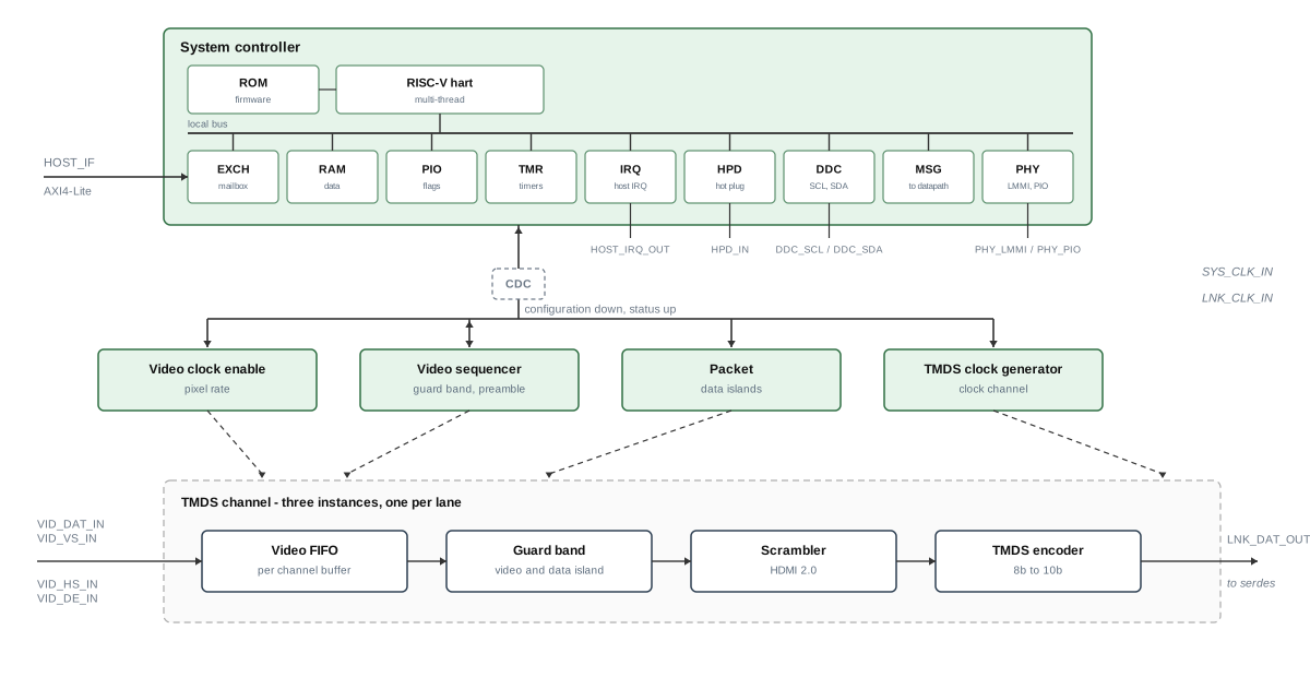
Figure 1: HDMI transmitter architecture (click on the image to enlarge it)
-
System controller
prt_hdmi_sc_topA RISC-V core with its own ROM and RAM, running the firmware that brings up and manages the link: hot plug detect, the DDC exchange with the sink, and the PHY controller. It talks to the application processor through a mailbox, and to the link layer through a message bus across the clock domain boundary.
-
Video FIFO
prt_hdmitx_vid_fifoOne per channel. It takes the video component for its own lane and buffers it, so that the sequencer can hand the datapath over between active video, the periods around it and the data islands without losing pixels.
-
Guard band
prt_hdmitx_gbInserts the video and data island guard bands, and merges the packet data coming from the packet block into the stream between the active video periods.
-
Scrambler
prt_hdmitx_tmds_scrmPerforms the scrambling required by the HDMI 2.0 specification. It is enabled by the system controller, together with the scrambler synchronization control period.
-
TMDS encoder
prt_hdmitx_tmds_encConverts each 8-bit character into its 10-bit TMDS symbol and drives the link data output towards the serdes.
-
Video sequencer
prt_hdmitx_vid_seqTracks where in the video period the link is and drives the preambles and guard bands that mark the transition between the video, control and data island periods.
-
Packet
prt_hdmitx_pktAssembles the data island packets, including their ECC, and offers them to the guard band block for insertion.
-
Oversampler
prt_hdmitx_ovsSends every bit two or four times, so that a format whose line rate falls below what the serdes can produce still gets on the wire. The link then runs at two or four times the rate the video needs, and each symbol occupies as many clocks. The width of the link path does not change; the repetition is in the time.
-
Link clock enable
prt_hdmitx_lnk_ckeProduces the one in one, one in two or one in four enable that the whole link domain runs on, so that the stages ahead of the oversampler only produce a symbol when there is a clock to send it in. One generator serves the three channels and the clock lane, so they cannot drift apart.
-
TMDS clock
prt_hdmitx_tmds_clkProduces the pattern for the fourth lane, the TMDS clock channel, at the ratio the current link rate asks for, and repeats its bits by the same factor the data lanes use. At the 1/40 ratio the pattern alternates per word, so leaving that repetition out would stop the clock lane from moving.
| Name | Type | Description | Values |
|---|---|---|---|
| P_VENDOR | String | Vendor | LSC |
| P_BEAT | Integer | Beat value | 50 |
| P_SPL | Integer | Symbols per lane | 2, 4 |
| P_PPC | Integer | Pixels per clock | 2, 4 |
| P_BPC | Integer | Bits per component | 8 |
| Name | Clock | Description | Width |
|---|---|---|---|
| SYS_RST_IN | SYS_CLK | System reset | 1 |
| SYS_CLK_IN | SYS_CLK | System clock (50 MHz) | 1 |
| HOST_IF | SYS_CLK | Host interface | AXI4-Lite |
| HOST_IRQ_OUT | SYS_CLK | Host interrupt | 1 |
| HPD_IN | SYS_CLK | Hot Plug Detect | 1 |
| HB_OUT | SYS_CLK | Heartbeat | 1 |
| DDC_SCL_INOUT | SYS_CLK | Display Data Communication Clock | 1 |
| DDC_SDA_INOUT | SYS_CLK | Display Data Communication Data | 1 |
| VID_VS_IN | LNK_CLK | Video vertical sync | P_PPC |
| VID_HS_IN | LNK_CLK | Video horizontal sync | P_PPC |
| VID_DAT_IN | LNK_CLK | Video data | 3 * P_PPC * P_BPC |
| VID_DE_IN | LNK_CLK | Video data enable | P_PPC |
| LNK_CLK_IN | LNK_CLK | Link clock | 1 |
| LNK_DAT_OUT | LNK_CLK | Link data | 4 * P_SPL * 10 |
Clocking
The core uses two clock domains. The system clock (SYS_CLK, 50 MHz) drives the system controller and the host interface (AXI4-Lite). The link clock (LNK_CLK) drives the video and link interfaces and is derived from the pixel clock divided by the number of pixels per clock. The video interface therefore runs synchronously with the link layer.
Video Interface
The HDMITX has a native video interface and supports 2 or 4 pixels per clock. The video interface signals listed in the signal table have the prefix VID_ and are high active. The video clock (VID_CLK_IN) runs at the pixel clock divided by the pixels per clock (2 or 4). For example with video resolution 1080p60 the pixel clock is 148.5 MHz. In 2 pixels per clock configuration the video clock runs at 74.25 MHz. It has a frequency of 37.125 MHz in 4 pixels per clock. The video clock must be stable and is generated by a PLL. The HDMITX can support any video timing as long as the horizontal video timing is dividable by the number of pixels per clock (2 or 4). The pixel mapping of the video interface for each supported color space (RGB 4:4:4, YCbCr 4:4:4 and YCbCr 4:2:2) is described in the HDMI Mapping section.
Link Interface
The link interface connects the HDMITX to the FPGA serdes. The link interface signals are prefixed with LNK_. The link clock (LNK_CLK_IN) is generated by the FPGA serdes and its frequency depends on the actual link rate. The link data (LNK_DAT_OUT) is directly routed to the FPGA serdes. See the HDMI reference design for the mapping.