Receiver
The DP receiver (DPRX) receives video from a DP source device. The core consists of two main layers; the policy maker (PM) and link layer (LNK).
The policy maker is responsible for communication with the upstream DP source device, training the link and controlling the link layer.
The link layer handles the (video) data transport.
The DPRX diagram is shown in figure 1.
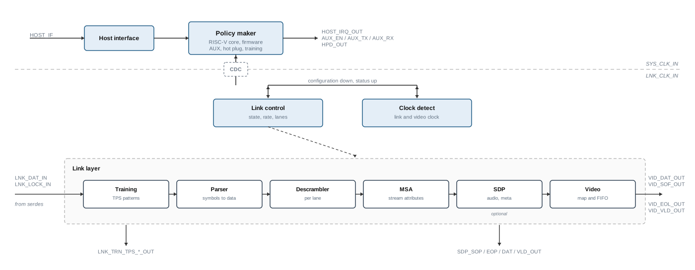
Figure 1: DPRX architecture (click on the image to enlarge it)
Architecture
The policy maker sits on the system clock. Everything below the clock domain boundary runs on the link clock. Link data from the FPGA serdes enters on the left and is unwound in the mirror image of the transmitter: training, parsing, descrambling, then the attributes and packets are lifted out and the pixels are mapped back onto the video interface. Link control drives every stage of the layer; the clock detectors only measure the incoming clocks and report what they find back to the policy maker.
-
Policy maker
prt_dp_pm_topA RISC-V core with its own ROM and RAM, running the firmware that owns the protocol: the AUX channel, the hot plug output, serving the capabilities to the source and link training. It talks to the application processor through a mailbox, and to the link layer through a message bus across the clock domain boundary.
-
Link control
prt_dprx_ctlHolds the link state the policy maker has set — line rate, lane count, transport mode — and drives the stages of the link layer accordingly.
-
Training
prt_dprx_trnRecognises the training pattern sequences the source sends while the link is being brought up and reports the result, so the policy maker can answer over the AUX channel. The pass and fail flags also leave the core directly.
-
Parser
prt_dprx_parsTurns the incoming symbols back into link data, separating the control symbols that frame the stream from the payload that follows them.
-
Descrambler
prt_dprx_scrmUndoes the scrambling on each lane and reports its lock state.
-
MSA
prt_dprx_msaRecovers the main stream attributes, the timing and format description of the picture the source is sending, and hands them to the policy maker.
-
SDP
prt_dprx_sdpLifts the secondary data packets carrying audio and meta data out of the stream and presents them on the secondary packet interface. Built in only when the SDP parameter is enabled.
-
Video
prt_dprx_vidMaps the lane data back into pixels, buffers them across into the video clock and drives the video interface.
| Name | Type | Description | Values |
|---|---|---|---|
| P_VENDOR | String | Vendor | AMD, ALTERA, LSC |
| P_BEAT | Integer | Beat value | 50 |
| P_SDP | Bool | SDP support | 0, 1 |
| P_LANES | Integer | Number of lanes | 2, 4 |
| P_SPL | Integer | Symbols per lane | 2, 4 |
| P_PPC | Integer | Pixels per clock | 2, 4 |
| P_BPC | Integer | Bits per component | 8, 10 |
| P_VID_DAT | Integer | Video data width | 48, 64, 96, 120 |
| Name | Clock | Description | Width |
|---|---|---|---|
| SYS_RST_IN | SYS_CLK | System reset | 1 |
| SYS_CLK_IN | SYS_CLK | System clock (50 MHz) | 1 |
| HOST_IF | SYS_CLK | Host interface | APB |
| HOST_IRQ_OUT | SYS_CLK | Host interrupt | 1 |
| AUX_EN_OUT | SYS_CLK | AUX channel enable | 1 |
| AUX_TX_OUT | SYS_CLK | AUX channel transmit | 1 |
| AUX_RX_IN | SYS_CLK | AUX channel receive | 1 |
| HPD_OUT | SYS_CLK | Hot Plug Detect | 1 |
| HB_OUT | SYS_CLK | Heartbeat | 1 |
| LNK_CLK_IN | LNK_CLK | Link clock | 1 |
| LNK_DAT_IN | LNK_CLK | Link data | P_LANES * P_SPL * 9 |
| LNK_SYNC_OUT | LNK_CLK | Link sync | 1 |
| LNK_VBID_OUT | LNK_CLK | Vertical Blanking ID | 1 |
| VID_CLK_IN | VID_CLK | Video clock | 1 |
| VID_RDY_IN | VID_CLK | Video ready | 1 |
| VID_SOF_OUT | VID_CLK | Video start of frame | 1 |
| VID_EOL_OUT | VID_CLK | Video end of line | 1 |
| VID_DAT_OUT | VID_CLK | Video data. Per pixel {B / Cb, R / Cr, G / Y} | P_VID_DAT |
| VID_VLD_OUT | VID_CLK | Video valid | 1 |
| SDP_CLK_IN | SDP_CLK | Secondary data packet clock | 1 |
| SDP_SOP_OUT | SDP_CLK | Secondary data packet start | 1 |
| SDP_EOP_OUT | SDP_CLK | Secondary data packet end | 1 |
| SDP_DAT_OUT | SDP_CLK | Secondary data packet data | 32 |
| SDP_VLD_OUT | SDP_CLK | Secondary data packet valid | 1 |
| LNK_TRN_TPS_CR_OUT | LNK_CLK | Link training TPS clock recovery sequence | 1 |
| LNK_TRN_TPS_EQ_OUT | LNK_CLK | Link training TPS equalization sequence | 1 |
| LNK_TRN_TPS_PASS_OUT | LNK_CLK | Link training TPS passed | 1 |
| LNK_TRN_TPS_FAIL_OUT | LNK_CLK | Link training TPS failed | 1 |
Link Interface (LNK)
The link interface connects the DPRX with the FPGA serdes. The link interface signals have the prefix LNK_. The link clock (LNK_CLK_IN) is generated by the FPGA serdes. The link clock frequency depends on the actual link rate. The link data (LNK_DAT_IN) is directly coming from the FPGA serdes. See the DP reference design for the mapping.
Link clocking
The link clock for the various link rates are shown in the table below. The link clock is generated by the FPGA serdes.
| Link rate | Symbols per clock | Link clock |
|---|---|---|
| RBR - 1.62 | 2 | 81 |
| RBR - 1.62 | 4 | 40.5 |
| HBR - 2.7 | 2 | 135 |
| HBR - 2.7 | 4 | 67.5 |
| HBR2 - 5.4 | 2 | 270 |
| HBR2 - 5.4 | 4 | 135 |
| HBR3 - 8.1 | 2 | 405 |
| HBR3 - 8.1 | 4 | 202.5 |
Video Interface (VID)
The DPRX has an AXI-stream video interface. The interface can support 2 or 4 pixels per clock. The video interface signals listed in the signal table have the prefix VID_. The video clock is driving the video interface. The video data output VID_DAT_OUT is P_VID_DAT bits wide and carries per pixel {B / Cb, R / Cr, G / Y}, with green / Y in the lowest bits. Pixel 0 is the first pixel of the group and sits in the lowest bits of the bus. RGB 4:4:4 and YCbCr 4:4:4 share the same bit layout: Cr takes the place of red, Y the place of green and Cb the place of blue. YCbCr 4:2:2 and YCbCr 4:2:0 are passed through as they arrive on the link: the DPRX cuts the component stream of every lane into groups of three components and puts them on the pixel fields of the bus. The figures show the resulting layout over four data words (Data 0 to Data 3). The YCbCr 4:2:2 layout is shown for 4 lanes. With 8 bits per component in a core built for 10 bits per component (P_BPC = 10), the components are MSB-aligned in each 10-bit field and the 2 lowest bits are zero. With 2 pixels per clock and 10 bits per component the bus is 64 bits wide; the upper 4 bits are zero. The diagrams below show the waveform and pixel mappings of the various configurations.

Figure 2: Video - waveform
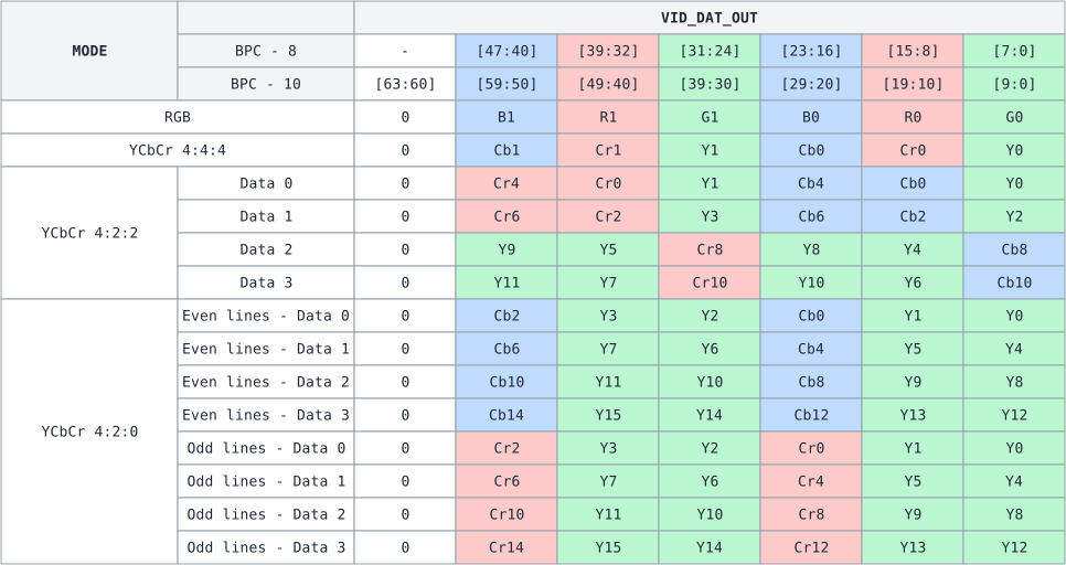
Figure 3: Video mapping - 2 pixels per clock (click on the image to enlarge it)
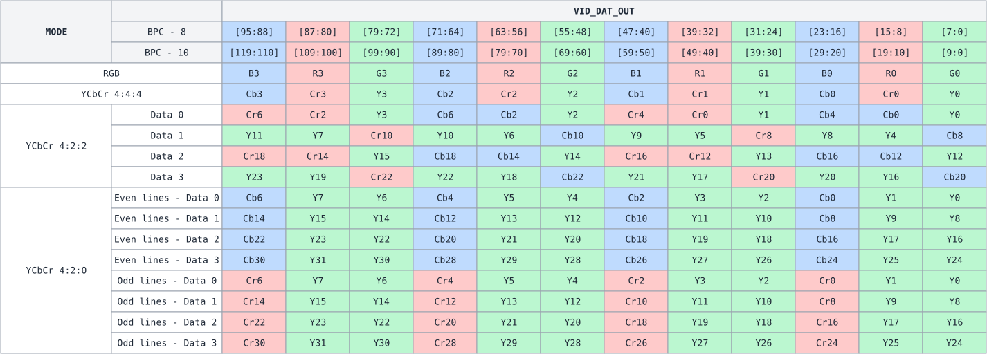
Figure 4: Video mapping - 4 pixels per clock (click on the image to enlarge it)
Video clocking
The video toolbox (VTB) module VTB uses the LNK_SYNC_OUT signal to recover the video clock. The external video clock generator (located on the Tentiva FMC board) generates the video clock and is steered by the VTB clock recovery module.
Secondary Data Packet Interface (SDP)
The DPRX handles all secondary data packets and output through the SDP interface.
The SDP interface signals listed in the signal table have the prefix SDP_. The SDP interface is running at a free running clock (SDP_CLK_IN).
The DPRX has an internal FIFO to store some SDP packets. To prevent the FIFO from overflowing, the SDP clock needs to run faster than the link clock.
Figure 5 provides a waveform diagram, showing the timing and mapping of the SDP signals for an infoframe.

Figure 5: SDP InfoFrame
Figure 6 shows the timing and mapping of a SDP audio packet.

Figure 6: SDP Audio Packet
Link training status (LNK_TRN_TPS)
The DPRX provides link training status signals that can be used for link training debugging.
The link training TPS clock recovery sequence signal and the link training TPS equalization sequence signal are updated when the DP source writes to the training pattern set (DPCD 0x00103). The signal LNK_TRN_TPS_CR_OUT is asserted when the DP source starts sending the clock recovery sequence (TPS1). When the DP source starts the equalization sequence (TPS2–TPS4), the signal LNK_TRN_TPS_EQ_OUT is asserted.
Both signals are deasserted when the DP source reads the lane training status (DPCD 0x00202). Depending on the training outcome, either LNK_TRN_TPS_PASS_OUT is asserted when the DPRX has detected a valid training pattern, or LNK_TRN_TPS_FAIL_OUT is asserted when the training pattern was not successfully detected.
The diagram in figure 7 shows the corresponding signal waveforms.
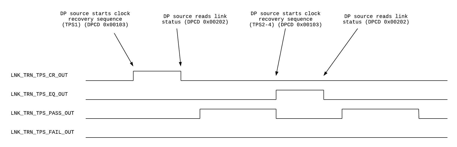
Figure 7: Link training status