Reference Design
Introduction
The reference design shows the HDMI TX (HDMITX) and HDMI RX (HDMIRX) IP-cores in a complete system. It consists of the HDMITX, the HDMIRX, the Video Pattern Generator (VPG), the PHY and the application. The VPG generates the colorbar test pattern and forwards the video of the HDMIRX in the pass-through.
The application runs on the processor of the FPGA vendor: the RISC-V MC soft processor of Lattice Propel on the Lattice FPGAs and the Arm Cortex-A55 of the hard processor system (HPS) on the Altera Agilex 5. The application processor runs the application code and the HDMI IP-core host driver (see Driver). It controls the IP-cores and the other peripherals through a memory mapped bus. The hot plug, DDC, EDID, SCDC and link handling are done by the system controller inside the HDMITX and HDMIRX IP-cores, so the application only handles the events of the IP-cores.
The reference design has two operation modes; colorbar and pass-through. In colorbar mode the test pattern, generated by the VPG, is transmitted by the HDMITX to the HDMI sink device. When a source is connected to the HDMI RX, the video coming from the HDMI source is captured by the HDMIRX and forwarded to the HDMITX through the VPG, in the video format of the source. The Agilex 5 reference design is a pass-through only, see below.
The Lattice reference designs use the Tentiva board. Tentiva is a video FMC board with HDMI sink and source connectors. Mount the Tentiva board on the FMC connector of the FPGA development board. Use the plastic screws to secure the Tentiva board. The Altera Agilex 5 modular development kit has HDMI connectors on the board and doesn't need the Tentiva.
The reference design is available for the following platforms;
- Lattice Avant Versa board (LAV-AT-X70)
- Lattice CertusPro-NX evaluation board
- Altera Agilex 5 E-Series 065A modular development kit
Console
The application has a menu on the UART. Open the serial port with a terminal program (115200 baud, 8N1). After start-up the application shows the version, loads the system controllers of the HDMITX and HDMIRX, writes the EDID of the HDMIRX, asserts the hot plug and prints the menu. The HDMI events (hot plug, link up / down, video up / down) are printed when they occur.
| Key | Command | Designs |
|---|---|---|
| q | HDMITX ping | All |
| e | HDMITX status | All |
| r | HDMITX read the EDID of the sink | All |
| a | HDMIRX ping | All |
| d | HDMIRX status | All |
| f | HDMIRX hot plug: unplug, plug or pulse | All |
| l | VPG video clock frequency | All |
| k | VPG scroller on or off | All |
| z | Colorbar. Select the video resolution | Lattice |
| b | Colorbar color depth (8 or 10 bits) | Lattice, 10-bit designs |
| y | Colorbar color space | Lattice |
| p | PHY status: lock, oversampling and the TMDS clock measured by the PHY | Altera |
Lattice Avant and CertusPro-NX
The Lattice reference design runs on two boards with the Tentiva on the FMC connector: the Avant Versa board (LAV-AT-X70-1LFG1156C) and the CertusPro-NX evaluation board (LFCPNX-100-9LFG672C). Both boards have the same design; the block diagram is shown below.
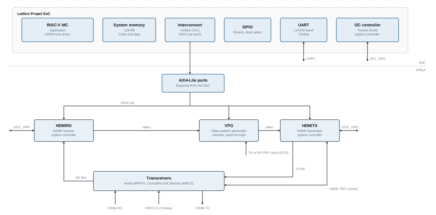
Figure 1: Lattice reference design
Processor
The application runs on the RISC-V MC soft processor of Lattice Propel, with a system memory of 128 KB. The UART, the I2C controller and a GPIO are Propel peripherals; the HDMITX, HDMIRX and VPG are connected through the AXI4-Lite ports of the Propel interconnect. The system clock is 50 MHz. The I2C controller configures the Tentiva (clock synthesizer and system controller).
| Address | Peripheral | Description |
|---|---|---|
| 0x1000_0000 | GPIO | Propel GPIO. HDMITX and HDMIRX reset, PHY clock select |
| 0x1000_2000 | HDMITX | HDMI transmitter |
| 0x1000_4000 | HDMIRX | HDMI receiver |
| 0x1000_6000 | VPG | Video pattern generator |
| 0x1100_0000 | I2C | Propel I2C controller (Tentiva) |
| 0x1200_0000 | UART | Propel UART (console) |
PHY
The transceivers are the MPPHY on the Avant and the SerDes (MPCS) on the CertusPro-NX, with the reference clock of the Tentiva. The PHY controller is part of the system controller of the HDMITX: it programs the line rate of the transceivers through the LMMI interface. In the pass-through the Tentiva forwards the TMDS clock of the HDMI source as the reference clock. Formats below the lowest line rate of the transceivers are sent and received with oversampling. A clock select (DCS) runs the HDMITX, the HDMIRX and the VPG on the TX clock of the PHY for the colorbar, and on the RX clock of the PHY for the pass-through.
| Board | Transceivers | Symbols per lane | Pixels per clock |
|---|---|---|---|
| Avant Versa | MPPHY | 2 | 2 |
| CertusPro-NX evaluation board | SerDes (MPCS) | 4 | 4 |
Build
The gateware is built with Lattice Radiant 2026.1, the application with Lattice Propel 2026.1. The steps are for the Avant, with the CertusPro-NX names in brackets.
- Gateware: in
gateware/synrunradiantc ../src/build_proj_lav.tcl(build_proj_lfcpnx.tcl). The script creates the Radiant project with the sources, the Lattice IP (system PLL and PHY) and the Propel SoChdmi_soc_lav(hdmi_soc_lfcpnx). Open the project in Radiant, regenerate the IP when Radiant asks for it, and run synthesis, map, place & route and the bitstream generation. - Application: start Propel SDK with the workspace
software/workspaceand build the projecthdmi_app.
Program
Program the bitstream over JTAG with the Radiant Programmer. Then load the application with the Propel SDK debugger: run or debug the project. The debugger loads the application into the system memory over JTAG and starts it. The application has to be loaded again after every power cycle.
Running on the Avant Versa and CertusPro-NX boards
Setup
- Mount the Tentiva on the FMC connector of the board.
- Connect the JTAG (USB) of the board to the host computer.
- Connect the UART (USB) of the Tentiva to the host computer.
- Connect an HDMI sink (monitor) to the HDMI TX connector and, for the pass-through, an HDMI source to the HDMI RX connector.
Altera Agilex 5 modular development kit
The reference design runs on the Agilex 5 E-Series 065A modular development kit (A5ED065AB32AE1V). The HDMI TX and RX connectors are on the carrier board. The block diagram is shown below.
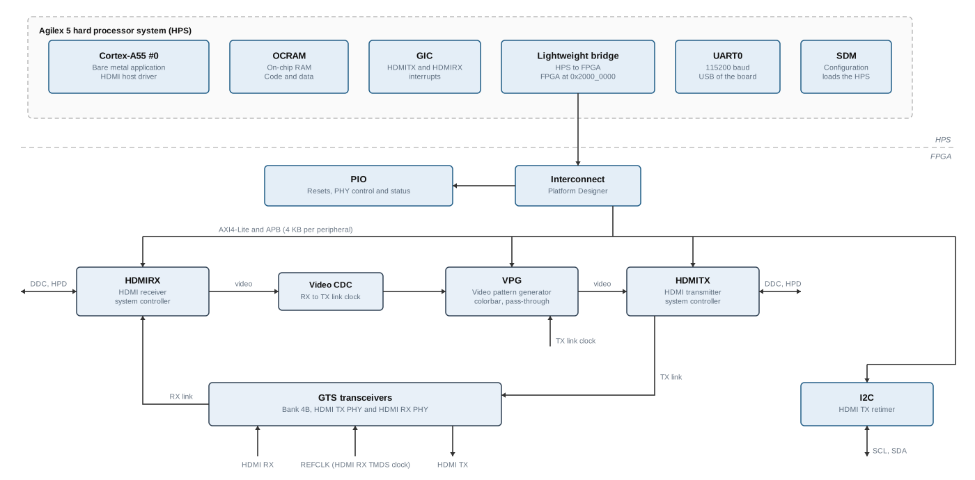
Figure 2: Altera Agilex 5 reference design
The reference clock of the HDMI TX transceivers is the TMDS clock of the HDMI RX connector, as in the Altera HDMI design example for this board. The HDMITX therefore only runs when a source is connected to the HDMI RX: the design is a pass-through. The HDMIRX receives TMDS clocks from 105 MHz up to HDMI 2.0 (5.94 Gbps, scrambled); tested are 1080p50, 1080p60, 2160p30, 2160p50 and 2160p60. Below 105 MHz the Altera HDMI RX PHY oversamples five times, which the HDMIRX does not support.
Hard processor system
The application runs bare metal on Cortex-A55 core 0 of the HPS, from the on-chip RAM (OCRAM). The application is the first stage boot loader: it is part of the bitstream, and the secure device manager (SDM) loads it after the FPGA is configured. The DDR memory is not used. The application initializes the HPS clocks and the interconnect itself. The console is HPS UART0. The interrupts of the HDMITX and HDMIRX go to the interrupt controller (GIC) of the HPS.
Programmable logic
The IP-cores and peripherals are connected to the lightweight HPS to FPGA bridge (Platform Designer). The system clock is 50 MHz.
| Address | Peripheral | Description |
|---|---|---|
| 0x2000_0040 | PIO out | PIO. HDMITX and HDMIRX reset, GTS system PLL start, HDMI TX PHY enable, TMDS bit clock ratio, HDMIRX locked |
| 0x2000_0050 | PIO in | PIO. Design parameters, PHY lock and oversampling, TMDS clock measured by the HDMI RX PHY |
| 0x2000_1000 | HDMITX | HDMI transmitter |
| 0x2000_2000 | HDMIRX | HDMI receiver |
| 0x2000_3000 | VPG | Video pattern generator |
| 0x2000_5000 | I2C | I2C controller (HDMI TX retimer TMDS1204) |
PHY
The PHY is the GTS transceiver bank 4B with the Altera HDMI TX PHY and HDMI RX PHY IP. The transmitters and the receivers share the four channels of the bank in a dual simplex group. The PHYs measure the TMDS clock and reconfigure the transceivers themselves; the application gives them the TMDS bit clock ratio, which the system controller of the HDMIRX reads from the SCDC. The datapaths of the transceivers run on the GTS system PLL (700 MHz from the 100 MHz reference clock of bank 4C). The HDMITX and HDMIRX have two symbols per lane and two pixels per clock at 8 bits per component. The HDMI TX PHY runs the transceivers at a multiple of the line rate; the HDMITX repeats the bits by the same factor. The transmitter and the receiver have their own link clock, so a video clock domain crossing takes the video of the HDMIRX over to the link clock of the HDMITX. The LED of the modular board is the system clock heartbeat (only when the FPGA is out of reset).
Setup
- Connect the USB port of the modular board to the host computer. It has the JTAG (USB-Blaster III) and the HPS UART.
- Connect an HDMI sink (monitor) to the HDMI TX connector and an HDMI source to the HDMI RX connector.
Build
The gateware is built with Quartus Prime Pro 26.1.1, the application with the Arm GNU toolchain 13.2 (aarch64-none-elf), cmake and ninja.
- Gateware: create the folder
gateware/syn/altera/ag5e_065a_mdkand run in itquartus_sh -t ../../../ref/altera/ag5e_065a_mdk/build_proj.tcl. The script creates the project, generates the Platform Designer system, the IP and the dual simplex group, and compiles the design. - Application:
software/build/app_ag5/build.sh. The script builds the system controller firmware and the application and adds the application to the bitstream (output_files/hdmi_ref_alt_ag5e_065a_mdk_hps.sof). The toolchain is downloaded when it is not installed.
Program
Program hdmi_ref_alt_ag5e_065a_mdk_hps.sof over JTAG with the Quartus Programmer. The FPGA is the second device in the JTAG chain, after the Arm DAP.
From the command line: quartus_pgm -c <cable> -m jtag -o "p;hdmi_ref_alt_ag5e_065a_mdk_hps.sof@2", where jtagconfig lists the cables.
The application starts after the configuration. When the HPS stops responding, power cycle the board.